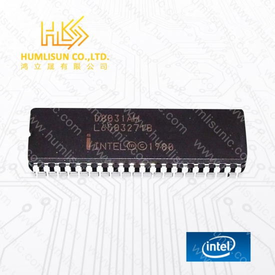
Part No .:
D8031AHManufacturer:
IntelDescription:
ICRemark:
new originLast Updated:
2026/06/30
Data sheet The Intel M2764A is a 5V only, 65,536-bit ultraviolet erasable and electrically programmable readonly memory (EPROM). The M2764A is an advanced version of the M2764 and is fabricated with Intel’s HMOSII-E technology which significantly reduces die size and greatly improves the device’s performance, power consumption, reliability, and producibility. The M2764A also offers reduced power consumption compared to the M2764. The maximum active current is 100 mA while the maximum standby current is only 40 mA. The standby mode lowers power consumption without increasing access time.
Data sheet Physical Case/Package CDIP Contact Plating Tin , Lead Number of Pins 24 Technical Conversion Rate 143 kS/s Differential Output No Integral Nonlinearity (INL) 0.75 LSB Interface Parallel Max Dual Supply Voltage 16.5 V Max Input Voltage 5 V Max Operating Temperature 125 °C Max Output Voltage 10 V Max Power Dissipation 450 mW Max Supply Voltage 16.5 V Min Dual Supply Voltage 10.8 V Min Input Voltage 5 V Min Operating Temperature -55 °C Min Output Voltage 5 V Min Supply Voltage 10.8 V Number of Bits 12 Number of Channels 1 Number of Converters 1 Number of D/A Converters 1 Number of DAC Channels 1 Output Type Voltage Polarity Bipolar , Unipolar Resolution 12 b Sampling Rate 143 kS/s Settling Time 7 µs Compliance Lead Free Contains Lead Radiation Hardening No RoHS Compliant DAC 1-CH R-2R 12-bit 24-Pin CDIP Tube
Data sheet Physical Case/Package N Number of Pins 16 Weight 0.037172 oz Technical Input Current 6 mA Max Operating Temperature 85 °C Min Operating Temperature -40 °C Operating Supply Current 6 mA Operating Supply Voltage 35 V Output Current 600 µA Dimensions Height 4.57 mm Length 19.3 mm Compliance Lead Free Lead Free Radiation Hardening No RoHS Compliant
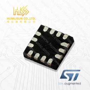
Data sheet Physical Case/Package LGA Contact Plating Nickel , Gold Number of Pins 14 Technical Axis X, Y, Z Bandwidth 5.3 kHz Interface I2C , SPI Max Operating Temperature 85 °C Max Supply Voltage 3.6 V Max Supply Voltage (DC) 3.6 V Min Operating Temperature -40 °C Min Supply Voltage 1.71 V Min Supply Voltage (DC) 1.71 V Operating Supply Current 2 µA Output Type Digital Sensor Type 3 Axis Dimensions Height 1 mm Length 2.15 mm Width 2.15 mm Compliance Lead Free Lead Free REACH SVHC No SVHC Radiation Hardening No RoHS Compliant MEMS digital output motion sensor: ultra low-power high performance 3-axis “femto” accelerometer Applications ■ Motion activated functions ■ Display orientation ■ Shake control ■ Pedometer ■ Gaming and virtual reality input devices ■ Impact recognition and logging
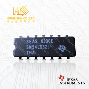
Data sheet Physical Case/Package CDIP Mount Through Hole Number of Pins 14 Technical High Level Output Current -400 µA Logic Function OR Low Level Output Current 4 mA Max Operating Temperature 125 °C Max Supply Voltage 5.5 V Min Operating Temperature -55 °C Min Supply Voltage 4.5 V Number of Bits 4 Number of Elements 4 Number of Gates 4 Number of Outputs 1 Operating Supply Voltage 5 V Output Type TTL Propagation Delay 22 ns Turn-On Delay Time 22 ns Compliance Lead Free Contains Lead Radiation Hardening No RoHS Compliant Quadruple 2-Input Positive-O Gates 14-CDIP -55 to 125
Data sheet Physical Case/Package QFN Mount Surface Mount Number of Pins 32 Technical Max Operating Temperature 85 °C Min Operating Temperature -40 °C Operating Supply Current 6 mA Compliance RoHS Compliant The AT73C213B is a fully integrated, low-cost, combined stereo audio DAC and audio power amplifier circuit targeted for Li-Ion or Ni-Mh battery powered devices such as mobile phones, smartphones, PDA, DECT phones, digital still cameras, music players or any other type of handheld device where an audio interface is needed. Power Management and Analog Companions (PMAAC) Audio Interface for Portable Handsets
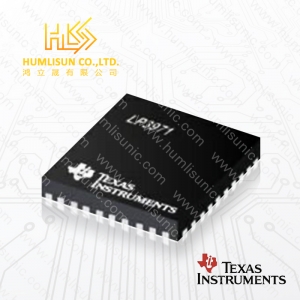
Data sheet Physical Mount Surface Mount Number of Pins 40 Technical Max Operating Temperature 125 °C Min Operating Temperature -40 °C Operating Supply Current 60 µA Dimensions Length 5 mm Compliance Lead Free Lead Free Radiation Hardening No RoHS Compliant Power Management IC (PMIC) for Advanced Application Processors 40-WQFN
Data sheet Physical Case/Package SOIC Mount Surface Mount Number of Pins 8 Technical Gain 6 dB Max Operating Temperature 85 °C Min Operating Temperature -40 °C Compliance Lead Free Lead Free Radiation Hardening No RoHS Compliant The MAX7450/MAX7451/MAX7452 complete front-end video-signal conditioners are designed to improve the quality of standard-definition video signals. The devices restore the DC level of the video input, correct for amplitude errors up to ±6dB, detect fault conditions, and filter out-of-band noise. The MAX7450/MAX7451/ MAX7452 optimize the signal quality for further video processing through a crosspoint switch or video decoder (ADC). Each device integrates an input video clamp, automatic gain control (AGC), loss-of-sync (LOS) detector, and an out-of-band noise/lowpass filter. These devices also incorporate a user-selectable buffer gain (0 or +6dB) and an AGC-disable function. The MAX7450 and MAX7451 operate from dual power supplies of ±5V or ±3.3V respectively, and they restore the video blanking level to GND. The MAX7452 operates from a single +5V supply and features a user-adjustable clamp level. The devices are available in an 8-pin SO package with an exposed pad and are specified for operation over the extended (-40°C to +85°C) temperature range.
Data Sheet Physical Case/Package SOT-70-6 Mount Surface Mount Weight 8.8E-05 oz Technical Bandwidth 100 MHz Max Operating Temperature 85 °C Max Supply Current 100 nA Max Supply Voltage 5.5 V Min Operating Temperature -40 °C Min Supply Voltage 1.65 V Number of Channels 1 On-State Resistance 1.1 Ω Operating Supply Current 100 nA Supply Type Single Throw Configuration SPDT Turn-Off Delay Time 15 ns Turn-On Delay Time 20 ns Compliance Lead Free Lead Free Radiation Hardening No RoHS Compliant The TS5A3159 device is a single-pole double-throw (SPDT) analog switch that is designed to operate from 1.65 V to 5.5 V. The device offers a low ON-state resistance and an excellent N-state resistance matching, with the break-before-make feature to prevent signal istortion during the transferring of a signal from one channel to another. The device has excellent total harmonic distortion (THD) performance and consumes very low power. These features make this device suitable for portable audio aplications.
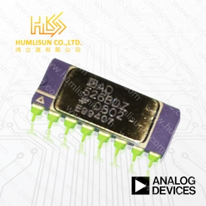
Data sheet Physical Case/Package CDIP Contact Plating Gold Mount Through Hole Number of Pins 16 Technical -3db Bandwidth 4 MHz Bandwidth 4 MHz Dual Supply Voltage 15 V Gain 16 dB Gain Bandwidth Product 100 kHz Input Bias Current 50 pA Input Offset Voltage (Vos) 700 µV Max Dual Supply Voltage 16.5 V Max Input Voltage 12 V Max Operating Temperature 125 °C Max Supply Voltage 16.5 V Min Dual Supply Voltage 4.5 V Min Operating Temperature -55 °C Min Supply Voltage 4.5 V Nominal Supply Current 10 mA Number of Amplifiers 1 Number of Channels 1 Number of Circuits 1 Number of Elements 1 Operating Supply Current 14 mA Output Current per Channel 10 mA Slew Rate 24 V/µs Dimensions Height 3.56 mm Length 21.34 mm Width 7.87 mm Compliance Lead Free Contains Lead REACH SVHC No SVHC Radiation Hardening No RoHS Compliant The AD526 is a single-ended, monolithic software programmable gain amplifier (SPGA) that provides gains of 1, 2, 4, 8 and 16. It is complete, including amplifier, resistor network and TTL-compatible latched inputs, and requires no external components. Low gain error and low nonlinearity make the AD526 ideal for precision instrumentation applications requiring programmable gain. The small signal bandwidth is 350 kHz at a gain of 16. In addition, the AD526 provides excellent dc precision. The FET-input stage results in a low bias current of 50 pA. A guaranteed maximum input offset voltage of 0.5 mV max (C grade) and low gain error (0.01%, G = 1, 2, 4, C grade) are accomplished using Analog Devices' laser trimming technology. To provide flexibility to the system designer, the AD526 can be operated in either latched or transparent mode. The force/sense configuration preserves accuracy when the output is connected to remote or low impedance loads. The AD526 is offered in one commercial (0°C to +70°C) grade, J, and three industrial grades, A, B and C, which are specified from -40°C to +85°C. The S grade is specified from -55°C to +125°C. The military version is available processed to MIL-STD 883B, Rev C. The J grade is supplied in a 16-pin plastic DIP, and the other grades are offered in a 16-pin hermetic side-brazed ceramic DIP.
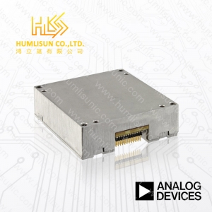
Data sheet Physical Case/Package Module Mount Panel Number of Pins 24 Technical -3db Bandwidth 330 Hz Max Operating Temperature 85 °C Max Supply Voltage 3.6 V Min Operating Temperature -40 °C Min Supply Voltage 3 V Nominal Supply Current 254 mA Operating Supply Current 254 mA Output Type SPI Sensor Type Accelerometer , Gyroscope , Magnetometer , 3 Axis Compliance Lead Free Contains Lead REACH SVHC No SVHC RoHS Compliant APPLICATIONS Platform stabilization and control Navigation Personnel tracking Instrumentation Robotics