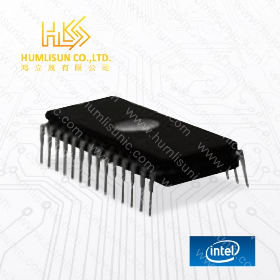
Part No .:
D2764AManufacturer:
IntelDescription:
ICRemark:
new originLast Updated:
2026/07/29
The Intel M2764A is a 5V only, 65,536-bit ultraviolet erasable and electrically programmable readonly memory (EPROM). The M2764A is an advanced version of the M2764 and is fabricated with Intel’s HMOSII-E technology which significantly reduces die size and greatly improves the device’s performance, power consumption, reliability, and producibility. The M2764A also offers reduced power consumption compared to the M2764. The maximum active current is 100 mA while the maximum standby current is only 40 mA. The standby mode lowers power consumption without increasing access time.
Data sheet Physical Case/Package SOIC Mount Surface Mount Number of Pins 8 Technical Gain 6 dB Max Operating Temperature 85 °C Min Operating Temperature -40 °C Compliance Lead Free Lead Free Radiation Hardening No RoHS Compliant The MAX7450/MAX7451/MAX7452 complete front-end video-signal conditioners are designed to improve the quality of standard-definition video signals. The devices restore the DC level of the video input, correct for amplitude errors up to ±6dB, detect fault conditions, and filter out-of-band noise. The MAX7450/MAX7451/ MAX7452 optimize the signal quality for further video processing through a crosspoint switch or video decoder (ADC). Each device integrates an input video clamp, automatic gain control (AGC), loss-of-sync (LOS) detector, and an out-of-band noise/lowpass filter. These devices also incorporate a user-selectable buffer gain (0 or +6dB) and an AGC-disable function. The MAX7450 and MAX7451 operate from dual power supplies of ±5V or ±3.3V respectively, and they restore the video blanking level to GND. The MAX7452 operates from a single +5V supply and features a user-adjustable clamp level. The devices are available in an 8-pin SO package with an exposed pad and are specified for operation over the extended (-40°C to +85°C) temperature range.
Data sheet Physical Contact Plating Copper , Tin , Silver Mount Surface Mount Technical Logic Function Receiver Max Operating Temperature 125 °C Min Operating Temperature -40 °C Operating Supply Current 2.5 A Compliance Lead Free Lead Free RoHS Compliant 5-W (WPC) Single-Chip Wireless Power Receiver with I2C 42-DSBGA -40 to 125
Data sheet Physical Case/Package DIP Mount Through Hole Number of Pins 16 Technical Drain to Source Resistance 10 Ω Dual Supply Voltage 9 V Max Dual Supply Voltage 20 V Max Operating Temperature 70 °C Max Power Dissipation 842 mW Max Supply Current 1 µA Max Supply Voltage 30 V Min Dual Supply Voltage 4.5 V Min Operating Temperature 0 °C Min Supply Voltage 4.5 V Nominal Supply Current 5 µA Number of Channels 4 On-State Resistance 10 Ω Operating Supply Voltage 18 V Supply Type Single , Dual Termination Through Hole Throw Configuration SPST Turn-Off Delay Time 235 ns Turn-On Delay Time 275 ns Dimensions Height 4.45 mm Length 19.43 mm Width 7.87 mm Compliance Lead Free Lead Free REACH SVHC Unknown Radiation Hardening No RoHS Compliant SWITCH, QUAD SPST, DIP16, 312; Switch Type, Analogue:SPST; Switches, No. of:4; Voltage, Supply Source:Dual; Resistance, On State:6.5ohm; Voltage, Supply Min:4.5V; Voltage, Supply Max:20V; Termination Type:Through Hole; Case Style:DIP; No. of Pins:16; Operating Temperature Range:0°C to +70°C; Base Number:312; IC Generic Number:312; Logic Function Number:312; No. of Channels:4; Resistance, Rds On:10ohm; Temp, Op. Max:70°C; Temp, Op. Min:0°C; Temperature Range, IC:Commercial
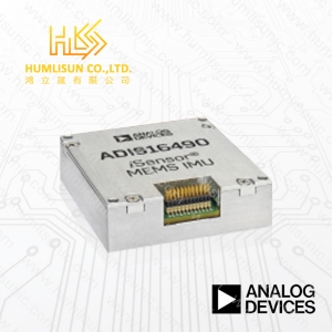
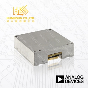
Physical Number of Pins 24 Compliance Lead Free Contains Lead RoHS Non-Compliant The ADIS16490 is a complete inertial system that includes a triaxis gyroscope and a triaxis accelerometer. Each inertial sensor in the ADIS16490 combines industry leading iMEMS® technology with signal conditioning that optimizes dynamic performance. The factory calibration characterizes each sensor for sensitivity, bias, alignment, and linear acceleration (gyroscope bias). As a result, each sensor has its own dynamic compensation formulas that provide accurate sensor measurements. The ADIS16490 provides a simple, cost effective method for integrating accurate, multiaxis inertial sensing into industrial systems, especially when compared with the complexity and investment associated with discrete designs. All necessary motion testing and calibration are part of the production process at the factory, greatly reducing system integration time. Tight orthogonal alignment simplifies inertial frame alignment in navigation systems. The SPI and register structure provide a simple interface for data collection and configuration control. The ADIS16490 uses the same footprint and connector system as the ADIS16375, ADIS16480, ADIS16485, and ADIS16488A, which greatly simplifies the upgrade process. The ADIS16490 is packaged in a module that is approximately 47 mm × 44 mm × 14 mm and includes a standard connector interface. Applications Precision instrumentation, stabilization Guidance, navigation, control Avionics, unmanned vehicles Precision autonomous machines, robotics
Data sheet Physical Case/Package CDIP Contact Plating Tin , Lead Mount Through Hole Number of Pins 14 Technical Common Mode Rejection Ratio 60 dB Input Bias Current 1 nA Input Offset Voltage (Vos) 2 mV Max Dual Supply Voltage 15 V Max Operating Temperature 125 °C Max Power Dissipation 1.2 W Max Supply Voltage 30 V Min Dual Supply Voltage 2.5 V Min Operating Temperature -55 °C Min Supply Voltage 5 V Nominal Supply Current 2 mA Number of Channels 4 Number of Elements 4 Output Current 16 mA Power Dissipation 1.2 W Power Supply Rejection Ratio (PSRR) 60 dB Response Time 5 µs Voltage Gain 93.98 dB Compliance Lead Free Contains Lead Radiation Hardening No RoHS Compliant Low Power Low Offset Voltage Quad Comparator 14-CDIP -55 to 125 Application areas include limit comparators, simple analog to digital converters; pulse, squarewave and time delay generators; wide range VCO; MOS clock timers; multivibrators and high voltage digital logic gates. The LM139 series was designed to directly interface with TTL and CMOS. When operated from both plus and minus power supplies, they will directly interface with MOS logic— where the low power drain of the LM139/LM139A is a distinct advantage over standard comparators.
Data sheet Physical Number of Pins 40 Technical Max Operating Temperature 85 °C Min Operating Temperature -40 °C Compliance RoHS Compliant High-Efficiency, Low-Iq, PMICs with Dynamic Voltage Management for Mobile Applica

Physical Case/Package TSSOP Mount Surface Mount Number of Pins 8 Weight 0.001411 oz Technical Frequency 105 kHz Max Frequency 105 kHz Max Operating Temperature 85 °C Max Supply Current 2.5 mA Max Supply Voltage 13.5 V Min Operating Temperature -40 °C Min Supply Voltage 3 V Nominal Supply Current 2.5 mA Operating Supply Current 1 mA Dimensions Height 1.15 mm Length 3 mm Width 4.4 mm Compliance Lead Free Contains Lead Radiation Hardening No RoHS Compliant Multi-topology Piezoelectric Transformer Controller 8-TSSOP
Data sheet Physical Contact Plating Gold Mount Surface Mount Number of Pins 8 Technical Density 1 Mb Frequency 15 MHz Interface Serial , 2-Wire Max Operating Temperature 85 °C Max Supply Voltage 5.5 V Memory Size 1 Mb Memory Type EEPROM Min Operating Temperature -40 °C Min Supply Voltage 3 V Nominal Supply Current 10 mA Voltage 5 V Compliance Lead Free Lead Free Radiation Hardening No RoHS Non-Compliant The AT17LV FPGA Configuration EEPROMs (Configurators) provide an easy-touse, cost-effective configuration memory solution for Field Programmable Gate Arrays. The AT17LV devices are packaged in the 8-lead LAP, 8-lead PDIP, 8-lead SOIC, 20-lead PLCC, 20-lead SOIC and 44-lead TQFP options(Table 1). The AT17LV Configurators use a simple serial-access procedure to configure one or more FPGA devices. The user can select the polarity of the reset function during programming. These devices also support a write protection mechanism within its programming mode.
Data sheet Physical Case/Package J Number of Pins 20 Technical Max Operating Temperature 125 °C Max Supply Voltage 20 V Min Operating Temperature -55 °C Number of Outputs 4 Output Current 500 A Switching Frequency 1 MHz Compliance Lead Free Contains Lead Radiation Hardening No RoHS Compliant
Data Sheet Physical Case/Package SOT-70-6 Mount Surface Mount Weight 8.8E-05 oz Technical Bandwidth 100 MHz Max Operating Temperature 85 °C Max Supply Current 100 nA Max Supply Voltage 5.5 V Min Operating Temperature -40 °C Min Supply Voltage 1.65 V Number of Channels 1 On-State Resistance 1.1 Ω Operating Supply Current 100 nA Supply Type Single Throw Configuration SPDT Turn-Off Delay Time 15 ns Turn-On Delay Time 20 ns Compliance Lead Free Lead Free Radiation Hardening No RoHS Compliant The TS5A3159 device is a single-pole double-throw (SPDT) analog switch that is designed to operate from 1.65 V to 5.5 V. The device offers a low ON-state resistance and an excellent N-state resistance matching, with the break-before-make feature to prevent signal istortion during the transferring of a signal from one channel to another. The device has excellent total harmonic distortion (THD) performance and consumes very low power. These features make this device suitable for portable audio aplications.