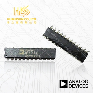
Part No .:
AT17LV010-10JIManufacturer:
AtmelDescription:
ICRemark:
new originLast Updated:
2026/07/19
|
Physical
|
|
| Case/Package | PLCC |
| Mount | Surface Mount |
| Number of Pins | 20 |
|
Technical
|
|
| Density | 1 Mb |
| Frequency | 15 MHz |
| Interface | Serial , 2-Wire |
| Max Operating Temperature | 85 °C |
| Max Supply Voltage | 5.5 V |
| Memory Size | 1 Mb |
| Memory Type | EEPROM |
| Min Operating Temperature | -40 °C |
| Min Supply Voltage | 3 V |
| Nominal Supply Current | 10 mA |
|
Compliance
|
|
| Lead Free | Contains Lead |
| Radiation Hardening | No |
| RoHS | Compliant |
The AT17LV series FPGA Configuration EEPROMs (Configurators) provide an easyto-use, cost-effective configuration memory for Field Programmable Gate Arrays. The AT17LV series device is packaged in the 8-lead LAP, 8-lead PDIP, 8-lead SOIC, 20- lead PLCC, 20-lead SOIC, 44-lead PLCC and 44-lead TQFP, see Table 1-1. The AT17LV series Configurators uses a simple serial-access procedure to configure one or more FPGA devices. The user can select the polarity of the reset function by programming four EEPROM bytes. These devices also support a write-protection mechanism within its programming mode. The AT17LV series configurators can be programmed with industry-standard programmers, Atmel’s ATDH2200E Programming Kit or Atmel’s ATDH2225 ISP Cable.
Data sheet Physical Case/Package PDIP Mount Through Hole Number of Pins 8 Technical Density 64 kb Frequency 12.5 MHz Interface Serial , 2-Wire Max Operating Temperature 85 °C Max Supply Voltage 5.5 V Memory Size 64 kb Memory Type EEPROM Min Operating Temperature -40 °C Min Supply Voltage 4.5 V The AT17LV series FPGA Configuration EEPROMs (Configurators) provide an easyto-use, cost-effective configuration memory for Field Programmable Gate Arrays. The AT17LV series device is packaged in the 8-lead LAP, 8-lead PDIP, 8-lead SOIC, 20- lead PLCC, 20-lead SOIC, 44-lead PLCC and 44-lead TQFP, see Table 1-1. The AT17LV series Configurators uses a simple serial-access procedure to configure one or more FPGA devices. The user can select the polarity of the reset function by programming four EEPROM bytes. These devices also support a write-protection mechanism within its programming mode.
Data sheet Physical Mount Surface Mount Number of Pins 8 Technical Density 8 Mb Frequency 33 MHz Interface Serial , 2-Wire Max Frequency 33 MHz Max Operating Temperature 85 °C Max Supply Voltage 3.63 V Memory Size 8 Mb Min Operating Temperature -40 °C Min Supply Voltage 2.97 V Nominal Supply Current 20 mA Operating Supply Current 20 mA Operating Supply Voltage 3.3 V Compliance Lead Free Contains Lead RoHS Non-Compliant The AT17F Series of In-System Programmable Configuration PROMs (Configurators) provide an easy-to-use, cost-effective configuration memory for Field Programmable Gate Arrays. The AT17F Series device is packaged in the 8-lead LAP, 20-lead PLCC, 44-lead PLCC and 44-lead TQFP, see Table 1-1. The AT17F Series Configurator uses a simple serial-access procedure to configure one or more FPGA devices. The AT17F Series Configurators can be programmed with industry-standard programmers, Atmel’s ATDH2200E Programming Kit or Atmel’s ATDH2225 ISP Cable. FPGA Configuration Flash Memory

Data sheet Physical Case/Package TQFP Number of Pins 44 Technical Max Frequency 33 MHz Max Operating Temperature 85 °C Max Supply Voltage 3.63 V Memory Size 8 Mb Min Operating Temperature -40 °C Min Supply Voltage 2.97 V Operating Supply Current 20 mA Compliance Lead Free Contains Lead RoHS Compliant The AT17F Series of In-System Programmable Configuration PROMs (Configurators) provide an easy-to-use, cost-effective configuration memory for Field Programmable Gate Arrays. The AT17F Series device is packaged in the 8-lead LAP, 20-lead PLCC, 44-lead PLCC and 44-lead TQFP, see Table 1-1. The AT17F Series Configurator uses a simple serial-access procedure to configure one or more FPGA devices. The AT17F Series Configurators can be programmed with industry-standard programmers, Atmel’s ATDH2200E Programming Kit or Atmel’s ATDH2225 ISP Cable.
Data sheet Physical Number of Pins 8 Technical Frequency 15 MHz Max Operating Temperature 85 °C Max Supply Voltage 5.5 V Memory Size 1 Mb Memory Type EEPROM Min Operating Temperature -40 °C Min Supply Voltage 4.5 V Nominal Supply Current 10 mA Compliance Lead Free Contains Lead RoHS Compliant The AT17LV series FPGA Configuration EEPROMs (Configurators) provide an easyto-use, cost-effective configuration memory for Field Programmable Gate Arrays. The AT17LV series device is packaged in the 8-lead LAP, 8-lead PDIP, 8-lead SOIC, 20- lead PLCC, 20-lead SOIC, 44-lead PLCC and 44-lead TQFP, see Table 1-1. The AT17LV series Configurators uses a simple serial-access procedure to configure one or more FPGA devices. The user can select the polarity of the reset function by programming four EEPROM bytes. These devices also support a write-protection mechanism within its programming mode. The AT17LV series configurators can be programmed with industry-standard programmers, Atmel’s ATDH2200E Programming Kit or Atmel’s ATDH2225 ISP Cable.
Data sheet Physical Case/Package PDIP Contact Plating Tin Mount Through Hole Number of Pins 8 Weight 0.032805 oz Technical Density 512 kb Interface Serial , 2-Wire Max Frequency 15 MHz Max Operating Temperature 85 °C Max Supply Voltage 5.5 V Memory Size 512 kb Memory Type EEPROM Min Operating Temperature -40 °C Min Supply Voltage 3 V Nominal Supply Current 10 mA Operating Supply Current 10 mA Compliance Lead Free Lead Free Radiation Hardening No RoHS Non-Compliant The Atmel® AT17LVxxxA FPGA configuration EEPROMs (Configurators) provide an easy-to-use, cost-effective configuration memory solution for FPGAs. The AT17LVxxxA are packaged in 8-lead PDIP and 20-lead PLCC options. The AT17LVxxxA configurator uses a simple serial-access procedure to configure one or more FPGA devices. The user can select the polarity of the reset function by programming four EEPROM bytes. These devices support a write protection mechanism within its programming mode.
Data sheet Physical Contact Plating Gold Mount Surface Mount Number of Pins 8 Technical Density 1 Mb Frequency 15 MHz Interface Serial , 2-Wire Max Operating Temperature 85 °C Max Supply Voltage 5.5 V Memory Size 1 Mb Memory Type EEPROM Min Operating Temperature -40 °C Min Supply Voltage 3 V Nominal Supply Current 10 mA Voltage 5 V Compliance Lead Free Lead Free Radiation Hardening No RoHS Non-Compliant The AT17LV FPGA Configuration EEPROMs (Configurators) provide an easy-touse, cost-effective configuration memory solution for Field Programmable Gate Arrays. The AT17LV devices are packaged in the 8-lead LAP, 8-lead PDIP, 8-lead SOIC, 20-lead PLCC, 20-lead SOIC and 44-lead TQFP options(Table 1). The AT17LV Configurators use a simple serial-access procedure to configure one or more FPGA devices. The user can select the polarity of the reset function during programming. These devices also support a write protection mechanism within its programming mode.
Data sheet Physical Case/Package LCC Mount Surface Mount Number of Pins 20 Technical Density 256 kb Frequency 12.5 MHz Interface Serial , 2-Wire Max Operating Temperature 85 °C Max Supply Voltage 5.5 V Memory Size 256 kb Memory Type EEPROM Min Operating Temperature -40 °C Min Supply Voltage 4.5 V Nominal Supply Current 10 mA Compliance Lead Free Contains Lead RoHS Compliant The AT17LV series FPGA Configuration EEPROMs (Configurators) provide an easyto-use, cost-effective configuration memory for Field Programmable Gate Arrays. The AT17LV series device is packaged in the 8-lead LAP, 8-lead PDIP, 8-lead SOIC, 20- lead PLCC, 20-lead SOIC, 44-lead PLCC and 44-lead TQFP, see Table 1-1. The AT17LV series Configurators uses a simple serial-access procedure to configure one or more FPGA devices. The user can select the polarity of the reset function by programming four EEPROM bytes. These devices also support a write-protection mechanism within its programming mode. The AT17LV series configurators can be programmed with industry-standard programmers, Atmel’s ATDH2200E Programming Kit or Atmel’s ATDH2225 ISP Cable.
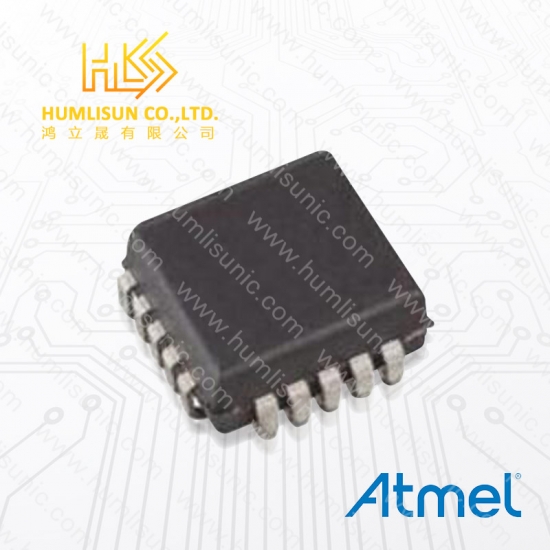
Data sheet Physical Case/Package QFN Mount Surface Mount Number of Pins 32 Technical Max Operating Temperature 85 °C Min Operating Temperature -40 °C Operating Supply Current 6 mA Compliance RoHS Compliant The AT73C213B is a fully integrated, low-cost, combined stereo audio DAC and audio power amplifier circuit targeted for Li-Ion or Ni-Mh battery powered devices such as mobile phones, smartphones, PDA, DECT phones, digital still cameras, music players or any other type of handheld device where an audio interface is needed. Power Management and Analog Companions (PMAAC) Audio Interface for Portable Handsets
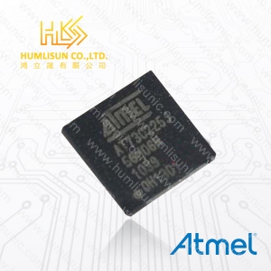
Data sheet Physical Mount PCB Technical Evaluation Kit Yes Interface SPI , Serial Operating Supply Voltage 3.3 V Sensor Type Accelerometer , Gyroscope , 3 Axis Compliance Lead Free Contains Lead REACH SVHC No SVHC RoHS Compliant The ADIS16445 iSensor® device is a complete inertial system that includes a triaxial gyroscope and a triaxial accelerometer. Each sensor in the ADIS16445 combines industry-leading iMEMS® technology with signal conditioning that optimizes dynamic performance. The factory calibration characterizes each sensor for sensitivity, bias, alignment, and linear accel-eration (gyroscope bias). As a result, each sensor has its own dynamic compensation formulas that provide accurate sensor measurements. The ADIS16445 provides a simple, cost-effective method for integrating accurate, multiaxis inertial sensing into industrial systems, especially when compared with the complexity and investment associated with discrete designs. All necessary motion testing and calibration are part of the production process at the factory, greatly reducing system integration time. Tight orthogonal alignment simplifies inertial frame alignment in navigation systems. The SPI and register structures provide a simple interface for data collection and configuration control. The ADIS16445 has a compatible pinout for systems that currently use other Analog Devices, Inc., IMU products, such as the ADIS16334 or the ADIS16485. Applications Platform stabilization and control Navigation Robotics
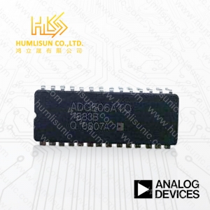
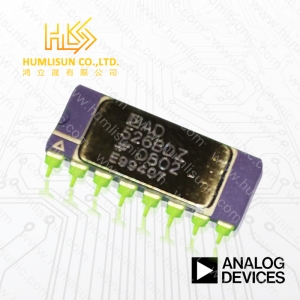
Data sheet Physical Case/Package CDIP Number of Pins 28 Technical Interface Parallel Max Dual Supply Voltage 16.5 V Max Operating Temperature 125 °C Max Power Dissipation 470 mW Max Supply Voltage 16.5 V Min Dual Supply Voltage 10.8 V Min Operating Temperature -55 °C Min Supply Voltage 10.8 V Nominal Supply Current 1.5 mA Number of Channels 1 Number of Inputs 16 Number of Outputs 1 On-State Resistance 700 Ω Operating Supply Voltage 15 V Propagation Delay 300 ns Supply Type Single , Dual Turn-Off Delay Time 450 ns Turn-On Delay Time 450 ns Compliance Lead Free Contains Lead Radiation Hardening No RoHS Compliant The ADG506A is a CMOS monolithic analog multiplexer with 16 channels. The ADG506A switches one of 16 inputs to a common output, depending on the state of four binary addresses and an enable input. It has TTL and 5 V CMOS logic compatible digital inputs. The ADG506A is designed on an enhanced LC2MOS process, which gives an increased signal capability of VSS to VDD and enables operation over a wide range of supply voltages. The devices can operate comfortably anywhere in the 10.8 V to 16.5 V single or dual supply range. This multiplexer also features high switching speeds and low RON.
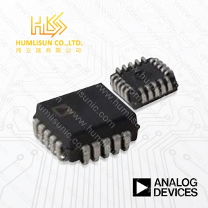
data sheet Physical Case/Package PLCC Contact Plating Tin Number of Pins 20 Technical Dual Supply Voltage 15 V High Level Output Current 30 mA Interface Parallel Max Dual Supply Voltage 22 V Max Operating Temperature 85 °C Max Power Dissipation 470 mW Max Supply Current 1 mA Max Supply Voltage 25 V Min Operating Temperature -40 °C Number of Bits 4 Number of Channels 4 Number of Circuits 4 Number of Inputs 4 Number of Outputs 4 On-State Resistance 115 Ω Operating Supply Voltage 5 V Polarity Non-Inverting Supply Type Dual Throw Configuration SPST Turn-Off Delay Time 450 ns Turn-On Delay Time 600 ns Dimensions Height 4.53 mm Length 8.89 mm Width 8.89 mm Compliance Lead Free Contains Lead RoHS Compliant The ADG211A is a monolithic CMOS device comprising four independently selectable switches. They are designed on an enhanced LC2MOS process which gives an increased signal handling capability of ±15 V. These switches also feature high switching speeds and low RON. The ADG211A switches are turned on with a logic low on the appropriate control input. Each switch conducts equally well in both directions when ON and each has an input signal range that extends to the supplies. All switches exhibit break-before-make switching action for use in multiplexer applications. Inherent in the design is low charge injection for minimum transients when switching the digital inputs.