Part No .:
AT17LV010-10CIManufacturer:
AtmelDescription:
ICRemark:
new originLast Updated:
2026/07/20
|
Physical
|
|
| Number of Pins | 8 |
|
Technical
|
|
| Frequency | 15 MHz |
| Max Operating Temperature | 85 °C |
| Max Supply Voltage | 5.5 V |
| Memory Size | 1 Mb |
| Memory Type | EEPROM |
| Min Operating Temperature | -40 °C |
| Min Supply Voltage | 4.5 V |
| Nominal Supply Current | 10 mA |
|
Compliance
|
|
| Lead Free | Contains Lead |
| RoHS | Compliant |
Data sheet Physical Case/Package PDIP Mount Through Hole Number of Pins 8 Technical Density 64 kb Frequency 12.5 MHz Interface Serial , 2-Wire Max Operating Temperature 85 °C Max Supply Voltage 5.5 V Memory Size 64 kb Memory Type EEPROM Min Operating Temperature -40 °C Min Supply Voltage 4.5 V The AT17LV series FPGA Configuration EEPROMs (Configurators) provide an easyto-use, cost-effective configuration memory for Field Programmable Gate Arrays. The AT17LV series device is packaged in the 8-lead LAP, 8-lead PDIP, 8-lead SOIC, 20- lead PLCC, 20-lead SOIC, 44-lead PLCC and 44-lead TQFP, see Table 1-1. The AT17LV series Configurators uses a simple serial-access procedure to configure one or more FPGA devices. The user can select the polarity of the reset function by programming four EEPROM bytes. These devices also support a write-protection mechanism within its programming mode.
Data sheet Physical Mount Surface Mount Number of Pins 8 Technical Density 8 Mb Frequency 33 MHz Interface Serial , 2-Wire Max Frequency 33 MHz Max Operating Temperature 85 °C Max Supply Voltage 3.63 V Memory Size 8 Mb Min Operating Temperature -40 °C Min Supply Voltage 2.97 V Nominal Supply Current 20 mA Operating Supply Current 20 mA Operating Supply Voltage 3.3 V Compliance Lead Free Contains Lead RoHS Non-Compliant The AT17F Series of In-System Programmable Configuration PROMs (Configurators) provide an easy-to-use, cost-effective configuration memory for Field Programmable Gate Arrays. The AT17F Series device is packaged in the 8-lead LAP, 20-lead PLCC, 44-lead PLCC and 44-lead TQFP, see Table 1-1. The AT17F Series Configurator uses a simple serial-access procedure to configure one or more FPGA devices. The AT17F Series Configurators can be programmed with industry-standard programmers, Atmel’s ATDH2200E Programming Kit or Atmel’s ATDH2225 ISP Cable. FPGA Configuration Flash Memory

Data sheet Physical Case/Package TQFP Number of Pins 44 Technical Max Frequency 33 MHz Max Operating Temperature 85 °C Max Supply Voltage 3.63 V Memory Size 8 Mb Min Operating Temperature -40 °C Min Supply Voltage 2.97 V Operating Supply Current 20 mA Compliance Lead Free Contains Lead RoHS Compliant The AT17F Series of In-System Programmable Configuration PROMs (Configurators) provide an easy-to-use, cost-effective configuration memory for Field Programmable Gate Arrays. The AT17F Series device is packaged in the 8-lead LAP, 20-lead PLCC, 44-lead PLCC and 44-lead TQFP, see Table 1-1. The AT17F Series Configurator uses a simple serial-access procedure to configure one or more FPGA devices. The AT17F Series Configurators can be programmed with industry-standard programmers, Atmel’s ATDH2200E Programming Kit or Atmel’s ATDH2225 ISP Cable.
Data sheet Physical Case/Package PDIP Contact Plating Tin Mount Through Hole Number of Pins 8 Weight 0.032805 oz Technical Density 512 kb Interface Serial , 2-Wire Max Frequency 15 MHz Max Operating Temperature 85 °C Max Supply Voltage 5.5 V Memory Size 512 kb Memory Type EEPROM Min Operating Temperature -40 °C Min Supply Voltage 3 V Nominal Supply Current 10 mA Operating Supply Current 10 mA Compliance Lead Free Lead Free Radiation Hardening No RoHS Non-Compliant The Atmel® AT17LVxxxA FPGA configuration EEPROMs (Configurators) provide an easy-to-use, cost-effective configuration memory solution for FPGAs. The AT17LVxxxA are packaged in 8-lead PDIP and 20-lead PLCC options. The AT17LVxxxA configurator uses a simple serial-access procedure to configure one or more FPGA devices. The user can select the polarity of the reset function by programming four EEPROM bytes. These devices support a write protection mechanism within its programming mode.
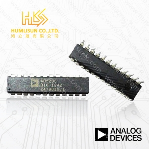
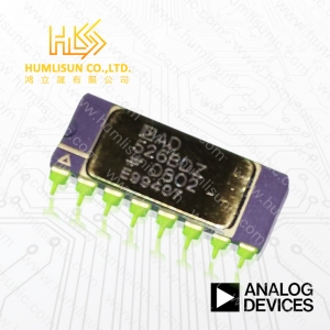
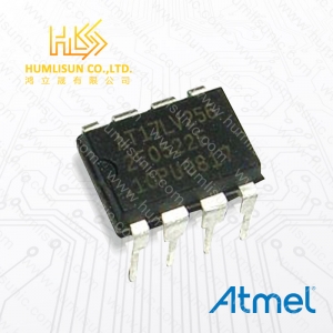
Data sheet Physical Contact Plating Gold Mount Surface Mount Number of Pins 8 Technical Density 1 Mb Frequency 15 MHz Interface Serial , 2-Wire Max Operating Temperature 85 °C Max Supply Voltage 5.5 V Memory Size 1 Mb Memory Type EEPROM Min Operating Temperature -40 °C Min Supply Voltage 3 V Nominal Supply Current 10 mA Voltage 5 V Compliance Lead Free Lead Free Radiation Hardening No RoHS Non-Compliant The AT17LV FPGA Configuration EEPROMs (Configurators) provide an easy-touse, cost-effective configuration memory solution for Field Programmable Gate Arrays. The AT17LV devices are packaged in the 8-lead LAP, 8-lead PDIP, 8-lead SOIC, 20-lead PLCC, 20-lead SOIC and 44-lead TQFP options(Table 1). The AT17LV Configurators use a simple serial-access procedure to configure one or more FPGA devices. The user can select the polarity of the reset function during programming. These devices also support a write protection mechanism within its programming mode.
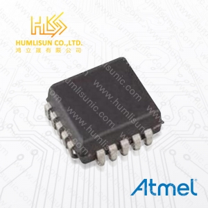
Data sheet Physical Case/Package PLCC Mount Surface Mount Number of Pins 20 Technical Density 1 Mb Frequency 15 MHz Interface Serial , 2-Wire Max Operating Temperature 85 °C Max Supply Voltage 5.5 V Memory Size 1 Mb Memory Type EEPROM Min Operating Temperature -40 °C Min Supply Voltage 3 V Nominal Supply Current 10 mA Compliance Lead Free Contains Lead Radiation Hardening No RoHS Compliant The AT17LV series FPGA Configuration EEPROMs (Configurators) provide an easyto-use, cost-effective configuration memory for Field Programmable Gate Arrays. The AT17LV series device is packaged in the 8-lead LAP, 8-lead PDIP, 8-lead SOIC, 20- lead PLCC, 20-lead SOIC, 44-lead PLCC and 44-lead TQFP, see Table 1-1. The AT17LV series Configurators uses a simple serial-access procedure to configure one or more FPGA devices. The user can select the polarity of the reset function by programming four EEPROM bytes. These devices also support a write-protection mechanism within its programming mode. The AT17LV series configurators can be programmed with industry-standard programmers, Atmel’s ATDH2200E Programming Kit or Atmel’s ATDH2225 ISP Cable.
Data sheet Physical Case/Package LCC Mount Surface Mount Number of Pins 20 Technical Density 256 kb Frequency 12.5 MHz Interface Serial , 2-Wire Max Operating Temperature 85 °C Max Supply Voltage 5.5 V Memory Size 256 kb Memory Type EEPROM Min Operating Temperature -40 °C Min Supply Voltage 4.5 V Nominal Supply Current 10 mA Compliance Lead Free Contains Lead RoHS Compliant The AT17LV series FPGA Configuration EEPROMs (Configurators) provide an easyto-use, cost-effective configuration memory for Field Programmable Gate Arrays. The AT17LV series device is packaged in the 8-lead LAP, 8-lead PDIP, 8-lead SOIC, 20- lead PLCC, 20-lead SOIC, 44-lead PLCC and 44-lead TQFP, see Table 1-1. The AT17LV series Configurators uses a simple serial-access procedure to configure one or more FPGA devices. The user can select the polarity of the reset function by programming four EEPROM bytes. These devices also support a write-protection mechanism within its programming mode. The AT17LV series configurators can be programmed with industry-standard programmers, Atmel’s ATDH2200E Programming Kit or Atmel’s ATDH2225 ISP Cable.
Data sheet Physical Case/Package QFN Mount Surface Mount Number of Pins 32 Technical Max Operating Temperature 85 °C Min Operating Temperature -40 °C Operating Supply Current 6 mA Compliance RoHS Compliant The AT73C213B is a fully integrated, low-cost, combined stereo audio DAC and audio power amplifier circuit targeted for Li-Ion or Ni-Mh battery powered devices such as mobile phones, smartphones, PDA, DECT phones, digital still cameras, music players or any other type of handheld device where an audio interface is needed. Power Management and Analog Companions (PMAAC) Audio Interface for Portable Handsets
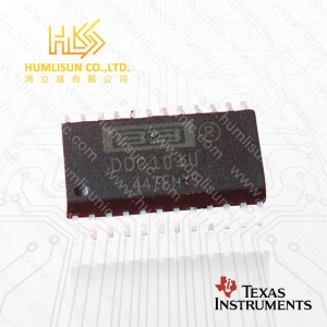
Data sheet Physical Case/Package SOIC Mount Surface Mount Number of Pins 24 Technical Conversion Rate 15 kS/s Dual Supply Voltage 5 V Interface SPI , Serial Max Dual Supply Voltage 5.25 V Max Operating Temperature 85 °C Min Dual Supply Voltage 4.75 V Min Operating Temperature -40 °C Number of A/D Converters 1 Number of Analog Inputs 1 Number of Bits 20 Number of Channels 1 Number of Converters 1 Number of Elements 1 Polarity Bipolar , Unipolar Resolution 20 b Sampling Rate 15 kS/s Supply Type Dual , Analog , Digital Compliance Lead Free Lead Free Radiation Hardening No RoHS Compliant 20-BIT ANALOG-TO-DIGITAL CONVERTER The DDC101 is a precision, wide dynamic range, charge digitizing A/D converter with 20-bit resolution. Lowlevel current output devices, such as photosensors, can bedirectly connected to its input. The most stringent accuracy requirements of many unipolar output sensor applications occur at low signal levels. To meet this requirement, Burr-Brown developed the adaptive delta odulation architecture of the DDC101 to provide linearly improving noise and linearity errors as the input signal level decreases. The DDC101 combines the functions of current-to-voltage conversion, integration, input programmable gain amplification, A/D conversion, and digital filtering to produce precision, wide dynamic range results. The input signal can be a low level current connected directly into the unit or a voltage connected through a user selected resistor. Although the DDC101 is optimized for unipolar signals, it can also accurately digitize bipolar input signals. The patented delta modulation topology combines charge integration and digitization functions. Oversampling and digital filtering reduce system noise dramatically. Correlated Double Sampling (CDS) captures and eliminates steady state and conversion cycle dependent offset and switching errors that are not eliminated with conventional analog circuits. The DDC101 block diagram is shown below. During conversion, the input signal is collected on the Internal integration capacitance for a user determined integration period. A high precision, autozeroed comparator samples the analog input node. Tracking logic updates the internal high resolution D/A converter at a 2MHz rate to maintain the analog input at virtual ground. A user programmable digital filter oversamples the tracking logic’s output. The digital filter passes a low noise, high resolution digital output to the serial I/O register. The serial outputs of multiple DDC101 units can be easily connected together in series or parallel if desired to minimize interconnections.
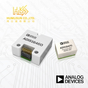
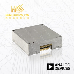
Data sheet Physical Case/Package Module Number of Pins 14 Technical Max Operating Temperature 85 °C Min Operating Temperature -25 °C Output Type SPI Sensor Type Accelerometer , Gyroscope , 6 Axis , Temperature Compliance Lead Free Contains Lead The ADIS16460 iSensor® device is a complete inertial system that includes a triaxial gyroscope and a triaxial accelerometer. Each sensor in the ADIS16460 combines industry leading iMEMS® technology with signal conditioning that optimizes dynamic performance. The factory calibration characterizes each sensor for sensitivity, bias, and alignment. As a result, each sensor has its own dynamic compensation formulas that provide accurate sensor measurements. The ADIS16460 provides a simple, cost effective method for integrating accurate, multiaxis inertial sensing into industrial systems, especially when compared with the complexity and investment associated with discrete designs. All necessary motion testing and calibration are part of the production process at the factory, greatly reducing system integration time. Tight orthogonal alignment simplifies inertial frame alignment in navigation systems. The SPI and register structures provide a simple interface for data collection and configuration control. The ADIS16460 is in an aluminum module package that is approximately 22.4 mm × 22.4 mm × 9 mm and has a 14-pin connector interface. Applications Smart agriculture/construction machinery Unmanned aerial vehicles (UAVs)/drones, and navigation and payload stabilization Robotics Factory/industrial automation personnel/asset tracking
Date sheet Physical Case/Package Module Mount Surface Mount Number of Pins 24 Technical Max Operating Temperature 125 °C Min Operating Temperature -40 °C Operating Supply Current 3.6 mA Compliance RoHS Compliant IC TFT PANEL MODULE 24-LLP