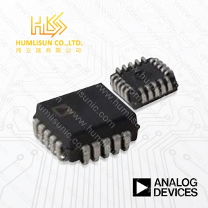
Part No .:
ADG333ABR-REELManufacturer:
Analog DevicesDescription:
ICRemark:
new originLast Updated:
2026/06/17
|
Physical
|
|
| Case/Package | SOIC W |
| Number of Pins | 20 |
|
Technical
|
|
| Dual Supply Voltage | 15 V |
| Interface | Parallel |
| Max Dual Supply Voltage | 20 V |
| Max Operating Temperature | 85 °C |
| Max Power Dissipation | 3.77 mW |
| Max Supply Current | 250 µA |
| Max Supply Voltage | 30 V |
| Min Dual Supply Voltage | 3 V |
| Min Operating Temperature | -40 °C |
| Min Supply Voltage | 3 V |
| Number of Bits | 4 |
| Number of Channels | 4 |
| Number of Circuits | 4 |
| Number of Inputs | 4 |
| Number of Outputs | 8 |
| On-State Resistance | 45 Ω |
| Operating Supply Current | 50 nA |
| Operating Supply Voltage | 12 V |
| Supply Type | Single , Dual |
| Test Frequency | 1 MHz |
| Throw Configuration | SPDT |
| Turn-Off Delay Time | 145 ns |
| Turn-On Delay Time | 175 ns |
|
Compliance
|
|
| Lead Free | Contains Lead |
| Radiation Hardening | No |
| RoHS | Compliant |
The ADG333A is a monolithic complementary metal-oxide semiconductor (CMOS) device comprising four independently selectable single-pole, double-throw (SPDT) switches. It is designed on a linear compatible CMOS (LC2MOS) process, which provides low power dissipation yet achieves a high switching speed and a low on resistance. The on-resistance profile is very flat over the full analog input range, ensuring good linearity and low distortion when switching audio signals. High switching speed also makes the device suitable for video signal switching. CMOS construction ensures ultralow power dissipation, making the device ideally suited for portable, battery-powered instruments. When they are on, each switch conducts equally well in both directions and has an input signal range that extends to the power supplies. In the off condition, signal levels up to the supplies are blocked. All switches exhibit break-before-make switching action for use in multiplexer applications. Low charge inject is inherent in the design. Product Highlights Extended signal range. The ADG333A is fabricated on an enhanced LC2MOS process, giving an increased signal range which extends to the supply rails. Low power dissipation. Low RON. Single-supply operation. For applications in which the analog signal is unipolar, the ADG333A can be operated from a single rail power supply. The device is fully specified with a single 12 V supply. Applications Audio and video switching Battery-powered systems Test equipment Communication systems
data sheet Physical Case/Package PLCC Contact Plating Tin Number of Pins 20 Technical Dual Supply Voltage 15 V High Level Output Current 30 mA Interface Parallel Max Dual Supply Voltage 22 V Max Operating Temperature 85 °C Max Power Dissipation 470 mW Max Supply Current 1 mA Max Supply Voltage 25 V Min Operating Temperature -40 °C Number of Bits 4 Number of Channels 4 Number of Circuits 4 Number of Inputs 4 Number of Outputs 4 On-State Resistance 115 Ω Operating Supply Voltage 5 V Polarity Non-Inverting Supply Type Dual Throw Configuration SPST Turn-Off Delay Time 450 ns Turn-On Delay Time 600 ns Dimensions Height 4.53 mm Length 8.89 mm Width 8.89 mm Compliance Lead Free Contains Lead RoHS Compliant The ADG211A is a monolithic CMOS device comprising four independently selectable switches. They are designed on an enhanced LC2MOS process which gives an increased signal handling capability of ±15 V. These switches also feature high switching speeds and low RON. The ADG211A switches are turned on with a logic low on the appropriate control input. Each switch conducts equally well in both directions when ON and each has an input signal range that extends to the supplies. All switches exhibit break-before-make switching action for use in multiplexer applications. Inherent in the design is low charge injection for minimum transients when switching the digital inputs.
Data sheet Physical Case/Package CDIP Number of Pins 28 Technical Interface Parallel Max Dual Supply Voltage 16.5 V Max Operating Temperature 125 °C Max Power Dissipation 470 mW Max Supply Voltage 16.5 V Min Dual Supply Voltage 10.8 V Min Operating Temperature -55 °C Min Supply Voltage 10.8 V Nominal Supply Current 1.5 mA Number of Channels 1 Number of Inputs 16 Number of Outputs 1 On-State Resistance 700 Ω Operating Supply Voltage 15 V Propagation Delay 300 ns Supply Type Single , Dual Turn-Off Delay Time 450 ns Turn-On Delay Time 450 ns Compliance Lead Free Contains Lead Radiation Hardening No RoHS Compliant The ADG506A is a CMOS monolithic analog multiplexer with 16 channels. The ADG506A switches one of 16 inputs to a common output, depending on the state of four binary addresses and an enable input. It has TTL and 5 V CMOS logic compatible digital inputs. The ADG506A is designed on an enhanced LC2MOS process, which gives an increased signal capability of VSS to VDD and enables operation over a wide range of supply voltages. The devices can operate comfortably anywhere in the 10.8 V to 16.5 V single or dual supply range. This multiplexer also features high switching speeds and low RON.
Data sheet Physical Case/Package SOIC Contact Plating Tin Number of Pins 24 Technical Conversion Rate 400 S/s Differential Output No Integral Nonlinearity (INL) 0.012 LSB Interface SPI , Serial Max Input Voltage 4.995 V Max Operating Temperature 85 °C Max Output Voltage 9.5 V Max Power Dissipation 176 mW Max Supply Voltage 32 V Min Input Voltage 5.005 V Min Operating Temperature -40 °C Min Output Voltage 29.5 V Min Supply Voltage 12 V Nominal Supply Current 4.2 mA Number of Bits 16 Number of Channels 1 Number of Converters 1 Number of D/A Converters 1 Number of DAC Channels 1 Number of Outputs 1 Output Type Voltage Polarity Unipolar , Bipolar Reference Voltage 5 V Resolution 16 b Sampling Rate 400 S/s Settling Time 2.5 ms Termination SMD/SMT Dimensions Height 2.65 mm Length 15.6 mm Width 7.6 mm Compliance Lead Free Contains Lead REACH SVHC No SVHC Radiation Hardening No RoHS Compliant The AD420 is a complete digital to current loop output converter, designed to meet the needs of the industrial control market. It provides a high precision, fully integrated, low cost single-chip solution for generating current loop signals in a compact 24-pin SOIC or PDIP package. The output current range can be programmed to 4 mA-20 mA, 0 mA-20 mA or an overrange function of 0 mA-24 mA. The AD420 can alternatively provide a voltage output from a separate pin that can be configured to provide 0 V-5 V, 0 V-10 V, ±5 V or ±10 V with the addition of a single external buffer amplifier. The 3.3 M Baud serial input logic design minimizes the cost of galvanic isolation and allows for simple connection to commonly used microprocessors. It can be used in three-wire or asynchronous mode and a serial-out pin is provided to allow daisy chaining of multiple DACs on the current loop side of the isolation barrier. The AD420 uses sigma-delta (SD) DAC technology to achieve 16-bit monotonicity at very low cost. Full-scale settling to 0.1% occurs within 3 ms. The only external components that are required (in addition to normal transient protection circuitry) are three low cost capacitors which are used in the DAC output filter. If the AD420 is going to be used at extreme temperatures and supply voltages, an external output transistor can be used to minimize power dissipation on the chip via the "BOOST" pin. The FAULT DETECT pin signals when an open circuit occurs in the loop. The on-chip voltage reference can be used to supply a precision +5 V to external components in addition to the AD420 or, if the user desires temperature stability exceeding 25 ppm/°C, an external precision reference such as the AD586 can be used as the reference. The AD420 is available in a 24-pin SOIC and PDIP over the industrial temperature range of -40°C to +85°C.
OP Amp Single GP ±18V 8-Pin CDIP Physical Case/Package CDIP Mount Through Hole Number of Pins 8 Technical Common Mode Rejection Ratio 140 dB Input Bias Current 2 nA Input Offset Voltage (Vos) 25 µV Max Dual Supply Voltage 22 V Max Operating Temperature 125 °C Min Dual Supply Voltage 3 V Min Operating Temperature -55 °C Number of Elements 1 Power Supply Rejection Ratio (PSRR) 123.1 dB Slew Rate 0.3 V/µs Voltage Gain 141.58 dB Compliance RoHS Non-Compliant
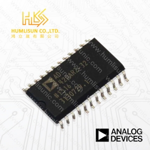
Data sheet Physical Case/Package SOIC W Contact Plating Tin Mount Surface Mount Number of Pins 24 Technical -3db Bandwidth 721 kHz Composition Potentiometer Dual Supply Voltage 2.5 V Interface SPI Max Dual Supply Voltage 2.7 V Max Operating Temperature 85 °C Max Supply Current 12 µA Max Supply Voltage 5.5 V Memory Type Volatile Min Dual Supply Voltage 2.3 V Min Operating Temperature -40 °C Min Supply Voltage 2.7 V Nominal Supply Current 12 µA Number of Circuits 6 Number of Elements 6 Number of Positions 256 Number of Taps 256 Operating Supply Current 12 µA Quiescent Current 12 µA Resistance 50 kΩ Taper Linear Temperature Coefficient 700 ppm/°C Tolerance 30% Dimensions Height 2.65 mm Length 15.6 mm Width 7.6 mm Compliance Lead Free Contains Lead REACH SVHC No SVHC RoHS Compliant The AD5204/AD5206 provide 4-/6-channel, 256-position digitally controlled variable resistor (VR) devices. These devices perform the same electronic adjustment function as a potentiometer or variable resistor. Each channel of the AD5204/ AD5206 contains a fixed resistor with a wiper contact that taps the fixed resistor value at a point determined by a digital code loaded into the SPI-compatible serial-input register. The resistance between the wiper and either endpoint of the fixed resistor varies linearly with respect to the digital code transferred into the VR latch. The variable resistor offers a completely programmable value of resistance between the A terminal and the wiper or the B terminal and the wiper. The fixed A-to-B terminal resistance of 10 kO, 50 kO, or 100 kO has a nominal temperature coefficient of 700 ppm/°C. Each VR has its own VR latch that holds its programmed resistance value. These VR latches are updated from an internal serial-to-parallel shift register that is loaded from a standard 3-wire serial-input digital interface. Eleven data bits make up the data-word clocked into the serial input register. The first three bits are decoded to determine which VR latch is loaded with the last eight bits of the data-word when the CS strobe is returned to logic high. A serial data output pin at the opposite end of the serial register (AD5204 only) allows simple daisy chaining in multiple VR applications without requiring additional external decoding logic. An optional reset (PR) pin forces all the AD5204 wipers to the midscale position by loading 0x80 into the VR latch. The AD5204/AD5206 are available in the 24-lead surface-mount SOIC, TSSOP, and PDIP packages. The AD5204 is also available in a 32-lead, 5 mm × 5 mm LFCSP package. All parts are guaranteed to operate over the extended industrial temperature range of -40°C to +85°C. For additional single-, dual-, and quad-channel devices, see the AD8400/AD8402/AD8403 data sheets. Applications Mechanical potentiometer replacement Instrumentation: gain, offset adjustment Programmable voltage-to-current conversion Programmable filters, delays, time constants Line impedance matching Data Sheet, Rev. B, 5/09
Data sheet Physical Case/Package CDIP Contact Plating Tin , Lead Number of Pins 24 Technical Conversion Rate 143 kS/s Differential Output No Integral Nonlinearity (INL) 0.75 LSB Interface Parallel Max Dual Supply Voltage 16.5 V Max Input Voltage 5 V Max Operating Temperature 125 °C Max Output Voltage 10 V Max Power Dissipation 450 mW Max Supply Voltage 16.5 V Min Dual Supply Voltage 10.8 V Min Input Voltage 5 V Min Operating Temperature -55 °C Min Output Voltage 5 V Min Supply Voltage 10.8 V Number of Bits 12 Number of Channels 1 Number of Converters 1 Number of D/A Converters 1 Number of DAC Channels 1 Output Type Voltage Polarity Bipolar , Unipolar Resolution 12 b Sampling Rate 143 kS/s Settling Time 7 µs Compliance Lead Free Contains Lead Radiation Hardening No RoHS Compliant DAC 1-CH R-2R 12-bit 24-Pin CDIP Tube
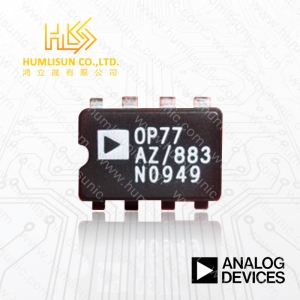
Data sheet Physical Case/Package Q Contact Plating Tin , Lead Number of Pins 8 Technical Common Mode Rejection Ratio 95 dB Gain Bandwidth Product 30 MHz Input Bias Current 3.3 µA Input Capacitance 1.5 pF Input Offset Voltage (Vos) 1 mV Input Voltage Noise Density 15 nV/sqrt Hz Max Dual Supply Voltage 18 V Max Operating Temperature 125 °C Max Power Dissipation 1.1 W Max Supply Voltage 36 V Min Dual Supply Voltage 4.5 V Min Operating Temperature -55 °C Min Supply Voltage 9 V Number of Amplifiers 1 Number of Channels 1 Number of Elements 1 Operating Supply Current 5.3 mA Power Dissipation 1.1 W Power Supply Rejection Ratio (PSRR) 86 dB Quiescent Current 4.8 mA Settling Time 120 ns Slew Rate 300 V/µs Unity Gain Bandwidth Product 35 MHz Voltage Gain 70.88 dB Compliance Lead Free Contains Lead Radiation Hardening No RoHS Compliant The AD847 represents a breakthrough in high speed amplifiers offing superior ac & dc perfomance and low power, all at low cost. The excellent dc performance is demonstrated by its ±5 V specifications which include an open-loop gain of 3500 V/V (500 Ohm load) and low input offset voltage of 0.5 mV. Common-mode rejection is a minimum of 78 dB. Output voltage swing is ±3 V into loads as low as 150 Ohm. Analog Devices also offers over 30 other high speed amplifiers from the low noise AD829 (1.7nV/(root)Hz) to the ultimate video amplifier, the AD811, which features 0.01% differential gain and 0.01° differential phase.
Data sheet Physical Case/Package CDIP Contact Plating Gold Mount Through Hole Number of Pins 16 Technical -3db Bandwidth 4 MHz Bandwidth 4 MHz Dual Supply Voltage 15 V Gain 16 dB Gain Bandwidth Product 100 kHz Input Bias Current 50 pA Input Offset Voltage (Vos) 700 µV Max Dual Supply Voltage 16.5 V Max Input Voltage 12 V Max Operating Temperature 125 °C Max Supply Voltage 16.5 V Min Dual Supply Voltage 4.5 V Min Operating Temperature -55 °C Min Supply Voltage 4.5 V Nominal Supply Current 10 mA Number of Amplifiers 1 Number of Channels 1 Number of Circuits 1 Number of Elements 1 Operating Supply Current 14 mA Output Current per Channel 10 mA Slew Rate 24 V/µs Dimensions Height 3.56 mm Length 21.34 mm Width 7.87 mm Compliance Lead Free Contains Lead REACH SVHC No SVHC Radiation Hardening No RoHS Compliant The AD526 is a single-ended, monolithic software programmable gain amplifier (SPGA) that provides gains of 1, 2, 4, 8 and 16. It is complete, including amplifier, resistor network and TTL-compatible latched inputs, and requires no external components. Low gain error and low nonlinearity make the AD526 ideal for precision instrumentation applications requiring programmable gain. The small signal bandwidth is 350 kHz at a gain of 16. In addition, the AD526 provides excellent dc precision. The FET-input stage results in a low bias current of 50 pA. A guaranteed maximum input offset voltage of 0.5 mV max (C grade) and low gain error (0.01%, G = 1, 2, 4, C grade) are accomplished using Analog Devices' laser trimming technology. To provide flexibility to the system designer, the AD526 can be operated in either latched or transparent mode. The force/sense configuration preserves accuracy when the output is connected to remote or low impedance loads. The AD526 is offered in one commercial (0°C to +70°C) grade, J, and three industrial grades, A, B and C, which are specified from -40°C to +85°C. The S grade is specified from -55°C to +125°C. The military version is available processed to MIL-STD 883B, Rev C. The J grade is supplied in a 16-pin plastic DIP, and the other grades are offered in a 16-pin hermetic side-brazed ceramic DIP.
Data sheet Physical Case/Package CDIP Mount Through Hole Number of Pins 8 Technical Common Mode Rejection Ratio 120 dB Input Offset Voltage (Vos) 90 µV Max Dual Supply Voltage 22 V Max Operating Temperature 85 °C Min Operating Temperature -40 °C Number of Elements 1 Power Dissipation 500 mW Power Supply Rejection Ratio (PSRR) 110 dB Slew Rate 0.3 V/µs Compliance RoHS Non-Compliant
Data sheet Physical Case/Package R Number of Pins 8 Technical Common Mode Rejection Ratio 110 dB Dual Supply Voltage 15 V Gain Bandwidth Product 75 kHz Input Bias Current 20 nA Input Offset Voltage (Vos) 500 µV Max Dual Supply Voltage 18 V Max Operating Temperature 125 °C Max Supply Voltage 36 V Min Dual Supply Voltage 1.5 V Min Operating Temperature -40 °C Min Supply Voltage 3 V Nominal Supply Current 300 µA Number of Amplifiers 2 Number of Channels 2 Number of Circuits 2 Number of Elements 2 Operating Supply Current 350 µA Operating Supply Voltage 28 V Output Current per Channel 25 mA Power Supply Rejection Ratio (PSRR) 110 dB Quiescent Current 150 µA Slew Rate 0.03 V/µs Unity Gain Bandwidth Product 75 kHz Voltage Gain 140 dB Compliance Lead Free Contains Lead Radiation Hardening No RoHS Compliant Rail-to-rail output swing combined with dc accuracy are the key features of the OP495 quad and OP295 dual CBCMOS operational amplifiers. By using a bipolar front end, lower noise and higher accuracy than those of CMOS designs have been achieved. Both input and output ranges include the negative supply, providing the user with zero-in/zero-out capability. For users of 3.3 V systems such as lithium batteries, the OP295/OP495 are specified for 3 V operation. Maximum offset voltage is specified at 300 µV for 5 V operation, and the open-loop gain is a minimum of 1000 V/mV. This yields performance that can be used to implement high accuracy systems, even in single-supply designs. The ability to swing rail-to-rail and supply 15 mA to the load makes the OP295/OP495 ideal drivers for power transistors and H bridges. This allows designs to achieve higher efficiencies and to transfer more power to the load than previously possible without the use of discrete components. For applications such as transformers that require driving inductive loads, increases in efficiency are also possible. Stability while driving capacitive loads is another benefit of this design over CMOS rail-to-rail amplifiers. This is useful for driving coax cable or large FET transistors. The OP295/OP495 are stable with loads in excess of 300 pF. The OP295 and OP495 are specified over the extended indus-trial (-40°C to +125°C) temperature range. The OP295 is available in 8-lead PDIP and 8-lead SOIC_N surface-mount packages. The OP495 is available in 14-lead PDIP and 16-lead SOIC_W surface-mount packages. Applications Battery-operated instrumentation Servo amplifiers Actuator drives Sensor conditioners Power supply control
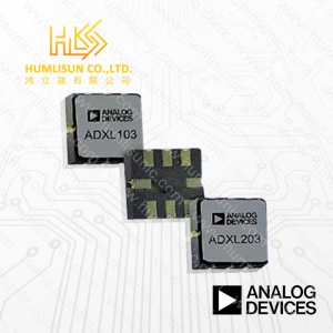
Data sheet Physical Case/Package LCC Contact Plating Nickel , Gold Number of Pins 8 Technical -3db Bandwidth 2.5 kHz Axis X, Y Bandwidth 0.5 Hz Frequency 5.5 kHz Max Operating Temperature 125 °C Max Supply Voltage 6 V Min Operating Temperature -40 °C Min Supply Voltage 3 V Nominal Supply Current 700 µA Operating Supply Current 700 µA Operating Supply Voltage 3.3 V Output Type Analog Sensitivity 1000 mV/g Dimensions Depth 5 mm Height 1.98 mm Length 5 mm Width 5 mm Compliance Lead Free Contains Lead REACH SVHC No SVHC Radiation Hardening No RoHS Compliant The ADXL103/ADXL203 are high precision, low power, complete single- and dual-axis accelerometers with signal conditioned voltage outputs, all on a single, monolithic IC. The ADXL103/ADXL203 measure acceleration with a full-scale range of ±1.7 g, ±5 g, ±18 g. The ADXL103/ADXL203 can measure both dynamic acceleration (for example, vibration) and static acceleration (for example, gravity). A typical noise floor as low as 110 µg/√Hz, allows signals below 1 mg (0.06° of inclination) to be resolved in tilt sensing applications using narrow bandwidths (<60 Hz). The user selects the bandwidth of the accelerometer using Capacitor CX and Capacitor CY at the XOUT and YOUT pins. Bandwidths of 0.5 Hz to 2.5 kHz may be selected to suit the application. The ADXL103 and ADXL203 are available in 5 mm × 5 mm × 2 mm, 8-pad hermetic LCC packages. Applications Vehicle dynamic control (VDC)/electronic stability program (ESP) systems Electronic chassis control Electronic braking Platform stabilization/leveling Navigation Alarms and motion detectors High accuracy, 2-axis tilt sensing